- 您现在的位置:买卖IC网 > Sheet目录345 > MT42L256M32D4KP-3 IT:A (Micron Technology Inc)IC LPDDR2 SDRAM 8GBIT 168FBGA
�� �
�
�2Gb:� x16,� x32� Mobile� LPDDR2� SDRAM� S4�
�Functional� Description�
�Functional� Description�
�Mobile� LPDDR2� is� a� high-speed� SDRAM� internally� configured� as� a� 4-� or� 8-bank� memory�
�device.� LPDDR2� devices� use� a� double� data� rate� architecture� on� the� command/address�
�(CA)� bus� to� reduce� the� number� of� input� pins� in� the� system.� The� 10-bit� CA� bus� is� used� to�
�transmit� command,� address,� and� bank� information.� Each� command� uses� one� clock� cy-�
�cle,� during� which� command� information� is� transferred� on� both� the� rising� and� falling�
�edges� of� the� clock.�
�LPDDR2-S4� devices� use� a� double� data� rate� architecture� on� the� DQ� pins� to� achieve� high-�
�speed� operation.� The� double� data� rate� architecture� is� essentially� a� 4� n� prefetch� architec-�
�ture� with� an� interface� designed� to� transfer� two� data� bits� per� DQ� every� clock� cycle� at� the�
�I/O� pins.� A� single� read� or� write� access� for� the� LPDDR2-S4� effectively� consists� of� a� single�
�4� n� -bit-wide,� one-clock-cycle� data� transfer� at� the� internal� SDRAM� core� and� four� corre-�
�sponding� n� -bit-wide,� one-half-clock-cycle� data� transfers� at� the� I/O� pins.�
�Read� and� write� accesses� are� burst� oriented;� accesses� start� at� a� selected� location� and�
�continue� for� a� programmed� number� of� locations� in� a� programmed� sequence.�
�Accesses� begin� with� the� registration� of� an� ACTIVATE� command� followed� by� a� READ� or�
�WRITE� command.� The� address� and� BA� bits� registered� coincident� with� the� ACTIVATE�
�command� are� used� to� select� the� row� and� bank� to� be� accessed.� The� address� bits� regis-�
�tered� coincident� with� the� READ� or� WRITE� command� are� used� to� select� the� bank� and� the�
�starting� column� location� for� the� burst� access.�
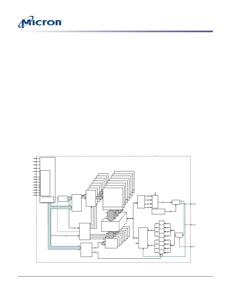
�Figure� 25:� Functional� Block� Diagram�
�CKE�
�CK�
�CK#�
�CS#�
�Control�
�logic�
�CA0�
�CA1�
�CA2�
�CA3�
�CA4�
�Bank� 7�
�Bank� 6�
�Bank� 5�
�Bank� 4�
�Bank� 7�
�Bank� 6�
�Bank� 5�
�Bank� 4�
�Bank� 3�
�CA5�
�CA6�
�CA7�
�CA8�
�CA9�
�Mode�
�registers�
�Refresh� x�
�counter�
�Row-�
�address�
�MUX�
�x�
�Bank� 3�
�Bank� 2�
�Bank� 1�
�Bank� 0�
�row-�
�address�
�latch�
�and�
�decoder�
�Bank� 2�
�Bank� 1�
�Bank� 0�
�Memory� array�
�4n�
�Read�
�latch�
�n�
�n�
�n�
�n�
�COL0�
�MUX�
�n�
�DATA�
�DRVRS�
�DQ0–DQn-1�
�Sense� amplifier�
�DQS�
�generator�
�DQS,� DQS#�
�4n�
�Input�
�registers�
�4�
�4�
�3�
�3�
�Bank�
�control�
�logic�
�I/O� gating�
�DM� mask� logic�
�4n�
�WRITE�
�FIFO�
�and�
�drivers�
�8�
�Mask�
�4�
�4�
�4�
�n�
�4�
�4�
�4�
�n�
�4�
�RCVRS�
�DQS,� DQS#�
�counter/�
�Column-� y� -� 1�
�address�
�1�
�Column�
�decoder�
�CK,� CK#�
�CK� out�
�CK� in�
�4n�
�Data�
�n�
�n�
�n�
�n�
�n�
�n�
�n�
�DM�
�latch�
�COL0�
�PDF:� 09005aef83f3f2eb�
�2gb_mobile_lpddr2_s4_g69a.pdf� –� Rev.� N� 3/12� EN�
�39�
�Micron� Technology,� Inc.� reserves� the� right� to� change� products� or� specifications� without� notice.�
�2010� Micron� Technology,� Inc.� All� rights� reserved.�
�发布紧急采购,3分钟左右您将得到回复。
相关PDF资料
MT45W1MW16BDGB-708 AT
IC PSRAM 16MBIT 104MHZ 54VFBGA
MT48H32M16LFB4-75B IT:C
IC SDRAM 512MB 54VFBGA
MT48H8M16LFB4-75 IT:K TR
IC SDRAM 128MBIT 133MHZ 54VFBGA
MTC100-JA2-P34
CONTACT INSERT PIN
MX841BE
IC CONVERTER WHITE LED 8-SOIC
MXHV9910BTR
IC LED DRIVER HIGH BRIGHT 8-SOIC
MXN12FB12F
MOTOR BRUSHED DC 12V 2922RPM
MXN13FB08B1
MOTOR BRUSHED DC 8V 4714RPM
相关代理商/技术参数
MT42L256M32D4KP-MS
制造商:Micron Technology Inc 功能描述:256MX32 LPDDR2 PLASTIC IND TEMP GREEN WFBGA 1.2V - Bulk